In today's post, the fourth in this series I start to look at some of the practical aspects of the Open Inverter design - starting with the proposed H-bridge and the choice of driver IC and heatsinks.
Sketching out the schematic, choosing the components and laying out the pcb is about 2 days work.
 |
| A typical N-FET H-Bridge with HIP4082 Driver IC and current sensing |
The circuit above shows a typical H-bridge arrangement based on N type FETs and a readily available H-bridge driver IC - the HIP4082 from Intersil.
The circuit will fit easily on a 5 x 5cm pcb, and with the correct choice of FETs - and heatsinks will handle 50V and 50A .
The FETs are in standard TO220 packages, and there is a wide range of FETs that could be selected depending on application.
The 2 main parameters for FET selection are the maximum Drain-Source voltage Vds, and the maximum Drain Current Id.
For safe operation at 48V it would be worth using 100V FETS, and 70A current handling - such as the Infineon 70N10.
It should be noted that the gates of the FETs contain a pair of resistors and a diode. These components limit the current supplied to the gate, control the turn on time and the diode improves the turn-off time. They also help protect the driver IC from damage and oscillation of the gate drive outputs.
The bill of materials for this H-bridge will be around £10 in 1 off.
 |
| The Intersil HIP4082 is an economical way to drive an N FET, H-bridge |
It should be a 1206 package or several resistors in parallel. 10A currents across 10 mOhm will dissipate 1W in the resistor. Special, precision metal current sense resistor links are available for this purpose. The gain of the op-amp should be chosen to suit the full scale input of the ADC on the microcontroller (typically 3V3 or 5V).
Typically the FETs will have about 10mOhm drain-source resistance when turned on. It is this RDSon that is the major dissipation of power in the FET. Remember that the power dissipation in the FET is the product of the square of the drain current Id and RDSon.
For example 20A passing through 10 mOhm will dissipate 4W in that FET, but 50A will dissipate 25W - and also 25W in the FET that forms the other active device in the H-bridge. The heatsink must me capable of removing this heat without the die of the FET overheating. A heatsink of about 3 degrees C per watt will be needed to safely handle these levels of heat dissipation.
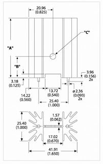
This one from Farnell (below) is fairly economical, and both the upper and lower FETs can be bolted to it - provided that they are insulated from each other and from the heatsink. The thermal performance is 2.6C per Watt provided the heatsink is placed vertically.
The heatsinks are quite chunky, and I have had to exploit the 17.02mm wide channel for the placement of the gate drive and current sensing components. Placing the two mosfets back to back can make for a reasonably compact arrangement.
 |
| Heatsink Farnell 1699368 has 2.6 C/W |
Putting it into Practice
 |
| First draft pcb layout in eagleCAD Size is 50mm x 50mm |
The layout proved to be quite tight, and a dual op-amp such as an LM358 might be preferable to the quad LM324 making a bit more room in the centre of the pcb.
Two heatsinks like the one shown in the drawing above are fitted. The heatsinks overhang the top and bottom edges of the pcb by about 10mm.
The outputs of the inverter (to the 24V- 230V transformer) are on the left. The battery or solar panel inputs are on the right.
A 10 way connector, PL1 allows the "Arduino" to be connected.
The connector in the centre of the right hand side is to accept an external capacitor C1, as only 1000uF at 50V will fit on the board.
As the driver chip runs on 12V, a 78M12 regulator in a TO252 package is included. Maximum voltage for this regulator is 35V.
4 comments:
One could also use this as a starting point to build a programmable AC power source. These AC sources are quite expensive, and are a necessary piece of test equipment when building things which are powered from the AC mains.
I'm only a hobbyish when it comes to electronics, but have I misunderstood something here?
This controller is for a 250W solar panel, but at full tilt the FETs are generating 50W of heat? That's 20% of the input? Surely that's not right?
Mark,
I was really just illustrating what the losses are in the FETs when they are driven hard at approaching their maximum drain current.
In the 250W application, the panel may typically be producing about 10A at 25V - so the I2R losses in the FETs will be (100 x 10 mOhm) which is only 1 watt. In these conditions the heatsink will be barely required.
However, I wanted to choose a heatsink that would cope with much higher powers - hence my 50A example.
Hello Ken,
it is possible to get your work - datas about this projekt?
I'm only a hobbyish and search a h-bridge for a dc-motors with 55V and Imax of 15A.
On my search I found your projekt inclusive a pcb of it, it wold be nice to get the Eagle files and Part list!
greetings from Germany MAT
Post a Comment